
The advantages of ASICs and highly integrated system-on-chip solutions in terms of cost reduction and increase in performance can be immense, and we believe WDC’s unique design-to-production flow offers you the lowest risk path to success.
We start with an extremely rigorous specification process. During the design phase itself, we use our extensive library of proven circuit IP to speed up projects, and build detailed design review and verification steps into all our designs – at specification, net list, layout and sample stages.
The Western Design Center can provide high-quality full custom ASIC development support and partnership
1.The ASIC design process begins from writing a functional description containing detailed requirements for the chip. We can start design on basis of a functional description prepared by the customer. Alternatively, we can create the functional description document based on the customer’s demands expressed in any form. At no time will we share your information with anyone without your explicit permission.
2.Based on your demands, our team estimates the amount of resources needed and produces a Statement of Work. After reaching an agreement, the actual work is started.
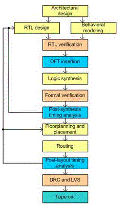
3.The first step is similar to FPGA design. The following tasks are run in parallel:
- Writing a synthesizable RTL (register transfer level) description (either on Verilog or VHDL) of the device.
- Writing a behavioral model, which is used to verify that the design meets its requirements.
- Writing a verification plan and a corresponding verification environment which describes and implements the method of proving the design correctness.
4.The RTL description is verified against the behavioral model by out dedicated Validation and Verification Department. This approach reduces the probability of the design error since no RTL designer tests his own code.
5.Most modern ASIC designs are complex enough to the stage when it’s impossible to tell apart valid chips from faulty at the production stage without special preparations during the design stages. These preparations are called DFT (design for test). DFT techniques include:
- Scan path insertion – a methodology of linking all registers into one long shift register (scan path). This can be used to check small parts of design instead of the whole design (the latter being almost always impossible).
- BIST (built-in self test) – a device used to check RAMs. After being triggered it feeds specific test patterns to the RAM module, reads back and compares results.
- ATPG (automatic test pattern generation) – a method of creating test vectors for scan paths and BIST automatically. Most modern EDA tool chains incorporate such a feature.
6.The synthesizable and verified RTL undergo logic synthesis. The synthesized reads RTL input, user-specified constraints and a cell library from the foundry. The output of the synthesis process is a gate-level netlist.
7.The netlist must undergo formal verification to prove that RTL and netlist are equivalent.
8.Preliminary timing results after synthesis are analyzed, critical paths are checked against the project performance requirements. If needed, the RTL description, constraints or synthesis options are modified, and the synthesis is repeated.
9.When timing constraints are finally met, the design proceeds to the layout, which consists of floor planning, placement and routing. Some other important tasks are performed at this step, including clock tree insertion.
10.Final (post-layout) timing results are again compared with performance requirements. If it doesn’t fit, the floor plan can be changed or placement run with other parameters.
11The last stage before tape out includes the following checks:
- DRC (design rule check) is a check that the layout conforms to the foundry-specific rules.
- LVS (layout versus schematic) is a formal equivalence check between the post-synthesis netlist and the final layout.
12.At last the resulting layout in GDSII format is handed to the semiconductor fabrication plant (foundry). This process is called tape out.