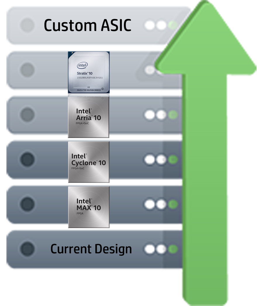
Scalability starting with the Intel® MAX® 10 FPGA:
WDC FPGA Supported Mods WDC FPGA Design Flow
 Intel® MAX® 10 FPGAs revolutionize non-volatile integration by delivering advanced processing capabilities in a low-cost, single-chip small form factor programmable logic device. Building upon the single-chip heritage of previous MAX device families, densities range from 2K – 50K LEs, using either single or dual-core voltage supplies. The MAX 10 FPGA family encompasses both advanced small wafer-scale packaging (3 mm x 3 mm) and high I/O pin count packages offerings.
MAX 10 FPGAs are built on TSMC’s 55 nm embedded NOR flash technology, enabling instant-on functionality. Integrated features include analog-to-digital converters (ADCs) and dual configuration flash allowing you to store and dynamically switch between two images on a single chip. MAX 10 FPGAs are built on TSMC’s 55 nm embedded NOR flash technology, enabling instant-on functionality. Integrated features include analog-to-digital converters (ADCs) and dual configuration flash allowing you to store and dynamically switch between two images on a single chip.
Scalability is key with choosing Intel® FPGAs. You can scale your design by migrating to more feature-rich offerings or if possible utilize your already implemented FPGA device to expand features to the current design. By starting with the MAX® 10 you start at the most cost-effective robust option in the market today.
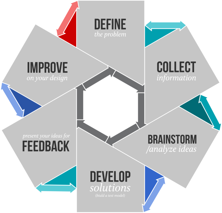
Speed to Market using an Agile Hardware Development Approach :
WDC’s Agile Hardware Development approach gives your hardware teams the flexibility to add and change features to meet the needs of the software development and verification teams. This enables each team to work independently while maintaining to work with a common goal identified. Alignment of project goals between device selection, RTL development, verification, and system software development are all in sync in such a way that features can be delivered in a proven modular fashion. Each team must be in lockstep with each other with a focus on the same system solution based goals. This incremental approach allows for feedback between teams much, sooner than would happen with traditional development. The feedback exchanged between teams is crucial to success, so that all teams are working toward the same goals simultaneously. The result gives way to opportunities to clarify design intent while holding far less potential for long schedule issues.
Effective completion dates early in the project, and the iterative approach should prove more likely and carry a higher degree of confidence in the end design. 
There are many potential values utilizing agile techniques which are appealing to FPGA-to-ASIC development approach.
Working within an Agile Hardware Development environment utilizing FPGA technology allows use an incremental feature development approach to your design requirements. Adaptive versions of the planning and development stages provide the opportunities to effectively analyze deliverables and modify design specifications to optimize deliverables and design intent, as a team.
Start working with WDC today!
For more information regarding FPGA-to-ASIC development with WDC technology please contact us at info@westerndesigncenter.com or by clicking the contact us button and filling out the form. This platform is for commercial use only.
Contact Us Form

