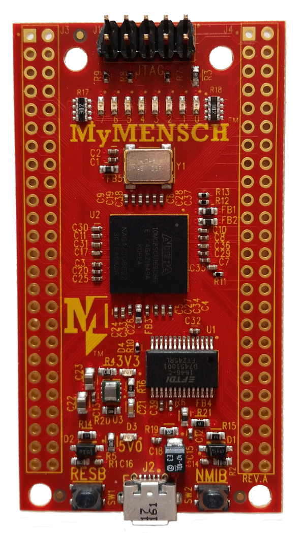
WDC Development Platform:
MyMENSCH™ Development Platform is the Western Design Center’s FPGA-to-ASIC™ (SBC), using a Programmable logic System on a Chip (PSoC) Intel PSG MAX10 10M08 FPGA.
The MyMENSCH™ Development Platform is built with technology from the most trusted name in the industry and leader in 65xx technology in conjunction with development partners.
This platform is available with our Microcontroller build W65C165i1 as a base build, however the option to customize the on board build to meet your unique requirements is available by contacting WDC. This agnostic system is flexible to meet all system requirements for development.
FPGA vs. ASIC Design Advantage
| FPGA Design | |
|---|---|
| Advantage | Benefit |
| Faster time-to-market | No layout, masks or other manufacturing steps are needed |
| No upfront non-recurring expenses (NRE) | Costs typically associated with an ASIC design |
| Simpler design cycle | Due to software that handles much of the routing, placement, and timing |
| More predictable project cycle | Due to elimination of potential re-spins, wafer capacities, etc. |
| Field reprogramability | A new bitstream can be uploaded remotely |
| ASIC Design | |
|---|---|
| Advantage | Benefit |
| Full custom capability | For design since device is manufactured to design specs |
| Lower unit costs | For very high volume designs |
| Smaller form factor | Since device is manufactured to design specs |
FPGA-to-ASIC Conversion Partnership
WDC has a long-term relationship with Progate Group Corporation (PGC) for ASIC manufacturing, testing and even FPGA-to-ASIC conversion.
PGC FPGA-to-ASIC Conversion

